


Hardware components | ||||||
| × | 1 | ||||
| × | 1 | ||||
| × | 1 | ||||
| × | 1 | ||||
Software apps and online services | ||||||
 |
| |||||
| ||||||
 |
| |||||
Modern society relies heavily on connectivity, making communication systems engineering a vital field. Unlike decades ago, when engineers worked in specialized silos—handling tasks like algorithm development, performance analysis, digital hardware implementation, or radio frequency front-end design—today’s engineers must master multiple skills. The rise of software-defined radio (SDR) has blurred these boundaries, requiring engineers to design algorithms and implement them on platforms like FPGAs or embedded devices, ending the era of isolated task silos.
This comprehensive tutorial serves as an accessible entry point into the world of Software-Defined Radios (SDRs). It provides step-by-step guidance on generating and receiving signals using SDR technology, while also demonstrating how to verify that the transmitted signal matches the intended output, ensuring accuracy and reliability in your SDR projects.
Introduction to Hardware KitsADRV9009ADRV9009 is a dual-channel RF transmitter and receiver. It also has two observation receivers. General charachteristics are shown in Figure 1. Detailed parameters can be seen from the devices datasheet available on internet.
The ZCU102 Evaluation Kit enables designers to jumpstart designs for automotive, industrial, video, and communications applications. This kit features an AMD Zynq™ UltraScale+™ MPSoC with a quad-core Arm® Cortex®-A53, dual-core Cortex-R5F real-time processors, and a Mali™-400 MP2 graphics processing unit based on 16nm FinFET+ programmable logic fabric by AMD. The ZCU102 supports all major peripherals and interfaces, enabling development for a wide range of applications.
DesignIn this tutorial, we will walk through the process of running an example design provided by Analog Devices. This design showcases the integration of the ADRV9009-W/PCBZ radio frequency (RF) transceiver evaluation board with the Xilinx ZCU102 evaluation board, connected via an FMC (FPGA Mezzanine Card) interface.
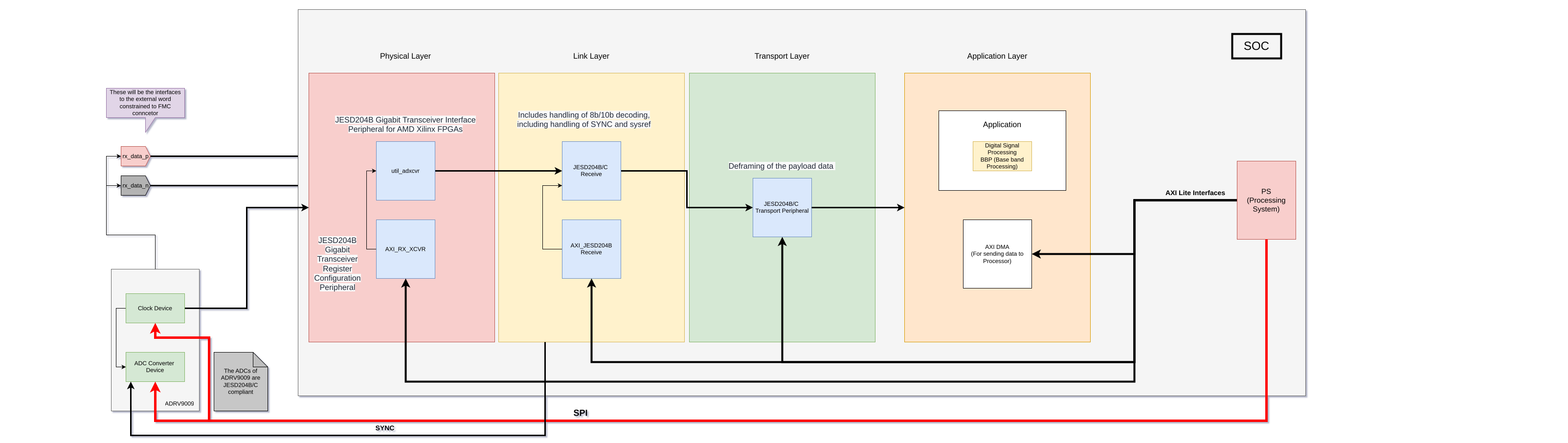
The setup demonstrates a high-performance RF front-end configuration commonly used in wireless communication and signal processing applications. A comprehensive system block diagram illustrating the interconnection between the ADRV9009 and ZCU102 boards is presented in Figure 2. This diagram will serve as a reference for understanding the data flow and the overall system architecture.
JESD204B High-Speed Data Interface
In this design, the JESD204B high-speed serial interface protocol is employed to facilitate data transmission between the ADRV9009 transceiver and the ZCU102 FPGA board. This protocol enables the transfer of high-throughput data streams from the onboard Analog-to-Digital Converters (ADCs) and Digital-to-Analog Converters (DACs) on the ADRV9009 to the FPGA for processing.
The ability to handle such high data rates is made possible by the inclusion of GTY transceivers in modern FPGAs. These high-speed serial transceivers support multi-gigabit communication, making them ideal for interfacing with high-performance RF front-end devices over the JESD204B protocol.
Figures 3 and 4 illustrate typical connection architectures between data converter boards (such as the ADRV9009) and the processing platform (ZCU102 FPGA). These diagrams provide insight into the physical and logical connectivity required for efficient high-speed data acquisition and transmission.
Step 1: Connect the ADRV9009 to the ZCU102
- Take the ADRV9009-W/PCBZ evaluation board and securely connect it to the HPC1 FMC (High-Pin Count) connector on the ZCU102 FPGA development board.
- Ensure the FMC connector is properly aligned and firmly seated to avoid signal integrity issues during operation.
Step 2: Connect the Transmit Channel to the Spectrum Analyzer
- Using a high-quality SMA (SubMiniature version A) coaxial cable, connect the TX1 output channel (Transmit Channel 1) on the ADRV9009 board to the input port of a spectrum analyzer
- The ADRV9009 is capable of operating up to at least 6 GHz, so make sure that your spectrum analyzer supports a frequency range of 6 GHz or higher to capture and analyze the transmitted signal accurately.
Note: Ensure that proper RF handling precautions are taken to prevent damage to equipment and to maintain signal fidelity.
Building HDLStep 3: Set Up the HDL Repository
Before proceeding with the design build and implementation, you must first set up the HDL (Hardware Description Language) repository from Analog Devices on your local machine. This repository contains the necessary source files, project scripts, and build infrastructure required for the FPGA design.
Follow the steps below to create a working directory and clone the HDL repository:
[~] mkdir adi
[~] cd adi
[~] git clone git@github.com:analogdevicesinc/hdl.gitNote:The git@github.com:format uses SSH for cloning. Make sure your Git environment is configured with an SSH key that is linked to your GitHub account.
Step 4: Building the Project Using Vivado
Once the HDL repository is set up, the next step is to build the FPGA project. This process involves running the implementation and synthesis flow using the Xilinx Vivado toolchain. The entire process is automated and can be initiated by following the below steps.
cd projects/adrv9009/zcu102
make
Be aware that this step may take a significant amount of time, as Vivado will execute multiple stages including IP generation, synthesis, implementation, and bitstream creation in the background.
After the build process completes successfully, navigate to the following directory:
cd projects/adrv9009/zcu102/adrv9009_zcu102.sdkIn this directory, you will find a file with the.xsa (Xilinx Support Archive) extension. This file contains all the hardware design information and is essential for the next phase—building the software application in Xilinx Vitis.
Note: The .xsa file replaces the older .hdf format in newer Vivado versions (2019.2 and later) and is used to hand off the hardware description to software development tools.
After successfully building the HDL project using the provided Makefile, Vivado automatically generates a complete hardware design, including synthesis and implementation results. You can now explore this design through the Vivado GUI.
Navigate to the project directory, typically located at:
~/adi/hdl/projects/adrv9009/zcu102Inside the project folder, locate the .xpr file. This is the Vivado project file that encapsulates all design settings, block diagrams, IP configurations, and synthesis/implementation results.
Once the project is open in Vivado:
- Use the Diagram view to examine the Block Design, including key IP cores like the JESD204 interface, GTY transceivers, clocking infrastructure, and data converters.
- Navigate to Implemented Design to inspect routing, timing, and resource utilization.
- Optionally, generate a Bitstream or re-run implementation if further changes are made.The design created during my workflow as shown in Figure 5.
It is difficult to explain the flow using this block diagram for this purpose I a have made an additional flow of signal for ease of understanding that is shown in Figure 6 & Figure 7 (Receive and Transmit Path Respectively).
Step 5: Build the Software Application Using Vitis
After generating the hardware description file (.xsa) from the HDL project, the next step is to develop the software application that will run on the Zynq Processing System (PS) of the ZCU102 board. This is done using Xilinx Vitis, the unified software development platform for embedded applications.
To begin, we will set up the no-OS (no operating system) software framework provided by Analog Devices, which contains reference software drivers and example projects tailored for their hardware platforms.
git clone --recursive https://github.com/analogdevicesinc/no-OSStep 6: Configure the Vitis Environment and Prepare for Software Build
To successfully build the software application using Xilinx Vitis, it is essential to ensure that the Vitis toolchain is correctly configured in your system environment.
6.1 Ensure Vitis is Accessible from the Command Line
Depending on your operating system, the process of setting up Vitis in your environment differs:
- On Windows:If Vitis is not automatically added to your system’s
PATH, you will need to manually add it via the System Environment Variables. This allows Vitis commands to be recognized from any terminal or command prompt. - On Linux:You can source the Vitis environment setup script directly. This script configures all the necessary environment variables to enable the use of Vitis tools in your current terminal session. Run the following command:
source /path/to/xilinx/Vitis/2024.2/settings64.shReplace /path/to/xilinx with the actual installation path where Vitis is installed on your system.
6.2 Copy the Hardware Description File (.xsa)
Next, copy the .xsa file generated in Step 4 (from the HDL build process) into the appropriate project directory within the no-OS repository. This .xsa file will be used as the hardware platform during the software build in Vitis.
For Example:
cp /path/to/hdl/projects/adrv9009/zcu102/adrv9009_zcu102.sdk/system_top.xsa ~/adi/no-OS/projects/adrv9009/Make sure to adjust the path to match the location of your .xsa file and cloned no-OS repository.
With the .xsa hardware description file in place and the Vitis environment properly configured, you are now ready to build the software application for the ADRV9009 + ZCU102 setup using the no-OS framework.
7.1 Navigate to the Project Directory
Change directory to the project folder where you previously copied the .xsa file:
cd ~/adi/no-OS/projects/adrv90097.2 Run the Build Commands
Execute the following commands to build the project:
# Clean any previous build artifacts (optional but recommended)
make clean

# Build the project using the Vitis toolchain
make
Now our project has been successfully build both on hardware and software side.
Running The ProjectStep 8: Launching and Modifying the Vitis Project
After successfully building the software using the Makefile, the next step is to launch the Vitis IDE to inspect and, if needed, modify the application code before deploying it to the hardware.
8.1 Launch Vitis
- Open Vitis Classic (or the standard Vitis IDE if you're not using the classic version).
- When prompted to select a workspace, choose the following directory:
~/adi/no-OS/projects/adrv9009- Do not create a new application project when prompted. Simply close the "Create Application Project" wizard.
Vitis will automatically detect the existing project files and metadata within the selected workspace directory.
8.2 Understanding and Modifying the Application
The default reference design included in the no-OS project is configured primarily for transmission (Tx) only. It transmits a signal for a short duration and then terminates execution. Reception (Rx) functionality is not included by default in the example project.
To extend the functionality of the application for your use case (e.g., continuous transmission or adding reception capability), you need to modify the main source file: headless.c.
This file is responsible for:
- Initializing system peripherals
- Configuring the ADRV9009 transceiver
- Starting the transmission process
- Managing runtime behavior (e.g., stopping, looping, or receiving)
In our case modification were made to headless.c for:
- Continuous transmission
- To receive data store it in memory has in hardware reception side is already conncted to a DMA which is further routed to the processor.
- Stream received that printing over UART. (For visualization in MATLAB)
headless.c File can be found in th projects folder: adrv9009/src/app and my version is as below:
/**
 * \file adrv9009/src/app/headless.c
 *
 * \brief Contains example code for user integration with their application
 *
 * Copyright 2015-2017 Analog Devices Inc.
 * Released under the AD9378-AD9379 API license, for more information see the "LICENSE.txt" file in this zip file.
 *
 */

/****< Insert User Includes Here >***/

#include <stdio.h>
#include "adi_hal.h"
#include "no_os_spi.h"
#include "no_os_error.h"
#include "no_os_delay.h"
#include "parameters.h"
#include "no_os_util.h"
#include "axi_dac_core.h"
#include "axi_adc_core.h"
#include "axi_dmac.h"
#ifndef ALTERA_PLATFORM
#include "xil_cache.h"
#include "xilinx_gpio.h"
#include "xilinx_spi.h"
#else
#include "altera_spi.h"
#include "altera_gpio.h"
#endif
#include "talise.h"
#include "talise_config.h"
#include "app_config.h"
#include "app_clocking.h"
#include "app_jesd.h"
#include "app_transceiver.h"
#include "app_talise.h"
#include "ad9528.h"
#define	 DMA_EXAMPLE
#ifdef IIO_SUPPORT

#include "iio.h"
#include "iio_app.h"
#include "iio_axi_adc.h"
#include "iio_axi_dac.h"
#ifndef ALTERA_PLATFORM
#include "xilinx_uart.h"
#else
#include "altera_uart.h"
#endif

int32_t start_iiod(struct axi_dmac *rx_dmac, struct axi_dmac *tx_dmac,
		   struct axi_adc *rx_adc, struct axi_dac *tx_dac)
{
	struct iio_axi_adc_init_param	iio_axi_adc_init_par;
	struct iio_axi_dac_init_param	iio_axi_dac_init_par;
	struct iio_app_init_param app_init_param = { 0 };
	struct iio_axi_adc_desc		*iio_axi_adc_desc;
	struct iio_axi_dac_desc		*iio_axi_dac_desc;
	struct iio_device		*adc_dev_desc;
	struct iio_device		*dac_dev_desc;
	struct iio_app_desc *app;
	int32_t				status;
	struct xil_uart_init_param platform_uart_init_par = {
#ifdef XPAR_XUARTLITE_NUM_INSTANCES
		.type = UART_PL,
#else
		.type = UART_PS,
		.irq_id = UART_IRQ_ID
#endif
	};

	struct no_os_uart_init_param iio_uart_ip = {
		.device_id = UART_DEVICE_ID,
		.irq_id = UART_IRQ_ID,
		.baud_rate = UART_BAUDRATE,
		.size = NO_OS_UART_CS_8,
		.parity = NO_OS_UART_PAR_NO,
		.stop = NO_OS_UART_STOP_1_BIT,
		.extra = &platform_uart_init_par,
		.platform_ops = &xil_uart_ops
	};

	iio_axi_adc_init_par = (struct iio_axi_adc_init_param) {
		.rx_adc = rx_adc,
		.rx_dmac = rx_dmac,
#ifndef PLATFORM_MB
		.dcache_invalidate_range = (void (*)(uint32_t,
						     uint32_t))Xil_DCacheInvalidateRange
#endif
	};

#ifndef ADRV9008_1
	iio_axi_dac_init_par = (struct iio_axi_dac_init_param) {
		.tx_dac = tx_dac,
		.tx_dmac = tx_dmac,
#ifndef PLATFORM_MB
		.dcache_flush_range = (void (*)(uint32_t, uint32_t))Xil_DCacheFlushRange,
#endif
	};
#endif

	status = iio_axi_adc_init(&iio_axi_adc_desc, &iio_axi_adc_init_par);
	if (status < 0)
		return status;

#ifndef ADRV9008_1
	status = iio_axi_dac_init(&iio_axi_dac_desc, &iio_axi_dac_init_par);
	if (status < 0)
		return status;
#endif

	iio_axi_adc_get_dev_descriptor(iio_axi_adc_desc, &adc_dev_desc);
#ifndef ADRV9008_1
	iio_axi_dac_get_dev_descriptor(iio_axi_dac_desc, &dac_dev_desc);
#endif

	struct iio_data_buffer read_buff = {
		.buff = (void *)ADC_DDR_BASEADDR,
		.size = 0xFFFFFFFF,
	};
#ifndef ADRV9008_1
	struct iio_data_buffer write_buff = {
		.buff = (void *)DAC_DDR_BASEADDR,
		.size = 0xFFFFFFFF,
	};
#endif

	struct iio_app_device devices[] = {
		IIO_APP_DEVICE("axi_adc", iio_axi_adc_desc, adc_dev_desc,
			       &read_buff, NULL, NULL),
#ifndef ADRV9008_1
		IIO_APP_DEVICE("axi_dac", iio_axi_dac_desc, dac_dev_desc,
			       NULL, &write_buff, NULL)
#endif
	};

	app_init_param.devices = devices;
	app_init_param.nb_devices = NO_OS_ARRAY_SIZE(devices);
	app_init_param.uart_init_params = iio_uart_ip;

	status = iio_app_init(&app, app_init_param);
	if (status)
		return status;

	return iio_app_run(app);
}

#endif // IIO_SUPPORT

/**********************************************************/
/**********************************************************/
/********** Talise Data Structure Initializations ********/
/**********************************************************/
/**********************************************************/

int main(void)
{
	adiHalErr_t err;
	int status;

	// compute the lane rate from profile settings
	// lane_rate = input_rate * M * 20 / L
	// 		where L and M are explained in taliseJesd204bFramerConfig_t comments
	uint32_t rx_lane_rate_khz = talInit.rx.rxProfile.rxOutputRate_kHz *
				    talInit.jesd204Settings.framerA.M * (20 /
						    no_os_hweight8(talInit.jesd204Settings.framerA.serializerLanesEnabled));
	uint32_t rx_div40_rate_hz = rx_lane_rate_khz * (1000 / 40);
	uint32_t tx_lane_rate_khz = talInit.tx.txProfile.txInputRate_kHz *
				    talInit.jesd204Settings.deframerA.M * (20 /
						    no_os_hweight8(talInit.jesd204Settings.deframerA.deserializerLanesEnabled));
	uint32_t tx_div40_rate_hz = tx_lane_rate_khz * (1000 / 40);
	uint32_t rx_os_lane_rate_khz = talInit.obsRx.orxProfile.orxOutputRate_kHz *
				       talInit.jesd204Settings.framerB.M * (20 /
						       no_os_hweight8(talInit.jesd204Settings.framerB.serializerLanesEnabled));
	uint32_t rx_os_div40_rate_hz = rx_os_lane_rate_khz * (1000 / 40);

	// compute the local multiframe clock
	// serializer:   lmfc_rate = (lane_rate * 100) / (K * F)
	// deserializer: lmfc_rate = (lane_rate * 100) / (K * 2 * M / L)
	// 		where K, F, L, M are explained in taliseJesd204bFramerConfig_t comments
	uint32_t rx_lmfc_rate = (rx_lane_rate_khz * 100) /
				(talInit.jesd204Settings.framerA.K * talInit.jesd204Settings.framerA.F);
	uint32_t tx_lmfc_rate = (tx_lane_rate_khz * 100) /
				(talInit.jesd204Settings.deframerA.K * 2 * talInit.jesd204Settings.deframerA.M /
				 no_os_hweight8(talInit.jesd204Settings.deframerA.deserializerLanesEnabled));
	uint32_t rx_os_lmfc_rate = (rx_os_lane_rate_khz * 100) /
				   (talInit.jesd204Settings.framerB.K * talInit.jesd204Settings.framerB.F);

	uint32_t lmfc_rate = no_os_min(rx_lmfc_rate, rx_os_lmfc_rate);
	lmfc_rate = no_os_min(tx_lmfc_rate, lmfc_rate);

	struct axi_adc_init rx_adc_init = {
		"rx_adc",
		RX_CORE_BASEADDR,
		TALISE_NUM_CHANNELS / 2
	};
	struct axi_adc *rx_adc;

	struct axi_adc_init rx_os_adc_init = {
		"rx_os_adc",
		RX_OS_CORE_BASEADDR,
		TALISE_NUM_CHANNELS / 2
	};
	struct axi_adc *rx_os_adc;

	struct axi_dac_init tx_dac_init = {
		"tx_dac",
		TX_CORE_BASEADDR,
		TALISE_NUM_CHANNELS,
		NULL,
		3
	};
	struct axi_dac *tx_dac;

	struct axi_dmac_init rx_dmac_init = {
		"rx_dmac",
		RX_DMA_BASEADDR,
		IRQ_DISABLED
	};
	struct axi_dmac *rx_dmac;

	struct axi_dmac_init rx_os_dmac_init = {
		"rx_os_dmac",
		RX_OS_DMA_BASEADDR,
		IRQ_DISABLED
	};
	struct axi_dmac *rx_os_dmac;

	struct axi_dmac_init tx_dmac_init = {
		"tx_dmac",
		TX_DMA_BASEADDR,
		IRQ_DISABLED
	};
	struct axi_dmac *tx_dmac;

#ifdef DMA_EXAMPLE
	struct no_os_gpio_desc *gpio_plddrbypass;
	struct no_os_gpio_init_param gpio_init_plddrbypass;
	extern const uint32_t sine_lut_iq[1024];
#endif
#ifndef ALTERA_PLATFORM
	struct xil_spi_init_param hal_spi_param = {
#ifdef PLATFORM_MB
		.type = SPI_PL,
#else
		.type = SPI_PS,
#endif
		.flags = SPI_CS_DECODE
	};
	struct xil_gpio_init_param hal_gpio_param = {
#ifdef PLATFORM_MB
		.type = GPIO_PL,
#else
		.type = GPIO_PS,
#endif
		.device_id = GPIO_DEVICE_ID
	};
#else
	struct altera_spi_init_param hal_spi_param = {
		.type = NIOS_II_SPI,
		.base_address = SPI_BASEADDR
	};
	struct altera_gpio_init_param hal_gpio_param = {
		.type = NIOS_II_GPIO,
		.device_id = 0,
		.base_address = GPIO_BASEADDR
	};

	hal.extra_gpio = &hal_gpio_param;
#endif
	int t;
	struct adi_hal hal[TALISE_DEVICE_ID_MAX];
	taliseDevice_t tal[TALISE_DEVICE_ID_MAX];
	for (t = TALISE_A; t < TALISE_DEVICE_ID_MAX; t++) {
		hal[t].extra_gpio = &hal_gpio_param;
		hal[t].extra_spi = &hal_spi_param;
		tal[t].devHalInfo = (void *) &hal[t];
	}
	hal[TALISE_A].gpio_adrv_resetb_num = TRX_A_RESETB_GPIO;
	hal[TALISE_A].spi_adrv_csn = ADRV_CS;
#if defined(ZU11EG) || defined(FMCOMMS8_ZCU102)
	hal[TALISE_B].gpio_adrv_resetb_num = TRX_B_RESETB_GPIO;
	hal[TALISE_B].spi_adrv_csn = ADRV_B_CS;
#endif

#ifndef ALTERA_PLATFORM
	/* Enable the instruction cache. */
	Xil_ICacheEnable();
	/* Enable the data cache. */
	Xil_DCacheEnable();
#endif

	printf("Hello\n");

	/**********************************************************/
	/**********************************************************/
	/************ Talise Initialization Sequence *************/
	/**********************************************************/
	/**********************************************************/

	err = clocking_init(rx_div40_rate_hz,
			    tx_div40_rate_hz,
			    rx_os_div40_rate_hz,
			    talInit.clocks.deviceClock_kHz,
			    lmfc_rate);
	if (err != ADIHAL_OK)
		goto error_0;

	err = jesd_init(rx_div40_rate_hz,
			tx_div40_rate_hz,
			rx_os_div40_rate_hz);
	if (err != ADIHAL_OK)
		goto error_1;

	err = fpga_xcvr_init(rx_lane_rate_khz,
			     tx_lane_rate_khz,
			     rx_os_lane_rate_khz,
			     talInit.clocks.deviceClock_kHz);
	if (err != ADIHAL_OK)
		goto error_2;

	for (t = TALISE_A; t < TALISE_DEVICE_ID_MAX; t++) {
		err = talise_setup(&tal[t], &talInit);
		if (err != ADIHAL_OK)
			goto error_3;
	}
#if defined(ZU11EG) || defined(FMCOMMS8_ZCU102)
	printf("Performing multi-chip synchronization...\n");
	for (int i = 0; i < 12; i++) {
		for (t = TALISE_A; t < TALISE_DEVICE_ID_MAX; t++) {
			err = talise_multi_chip_sync(&tal[t], i);
			if (err != ADIHAL_OK)
				goto error_3;
		}
	}
#endif
	ADIHAL_sysrefReq(tal[TALISE_A].devHalInfo, SYSREF_CONT_ON);

	jesd_rx_watchdog();

	/* Print JESD status */
	jesd_status();

	/* Initialize the DAC core */
#ifndef ADRV9008_1
	status = axi_dac_init(&tx_dac, &tx_dac_init);
	if (status) {
		printf("axi_dac_init() failed with status %d\n", status);
		goto error_3;
	}
#endif

	/* Initialize the ADC core */
#ifndef ADRV9008_2
	status = axi_adc_init(&rx_adc, &rx_adc_init);
	if (status) {
		printf("axi_adc_init() failed with status %d\n", status);
		goto error_3;
	}

#endif

#ifndef ADRV9008_1
	status = axi_adc_init(&rx_os_adc, &rx_os_adc_init);
	if (status) {
		printf("OBS axi_adc_init() failed with status %d\n", status);
		goto error_3;
	}

	status = axi_dmac_init(&tx_dmac, &tx_dmac_init);
	if (status) {
		printf("axi_dmac_init() tx init error: %d\n", status);
		goto error_3;
	}

#endif
#ifndef ADRV9008_2
	status = axi_dmac_init(&rx_dmac, &rx_dmac_init);
	if (status) {
		printf("axi_dmac_init() rx init error: %d\n", status);
		goto error_3;
	}
#endif

	status = axi_dmac_init(&rx_os_dmac, &rx_os_dmac_init);
	if (status) {
		printf("OBS axi_dmac_init() rx init error: %d\n", status);
		goto error_3;
	}

#ifdef DMA_EXAMPLE
	gpio_init_plddrbypass.extra = &hal_gpio_param;
#ifndef ALTERA_PLATFORM
	gpio_init_plddrbypass.platform_ops = &xil_gpio_ops;
#else
	gpio_init_plddrbypass.platform_ops = &altera_gpio_ops;
#endif
	gpio_init_plddrbypass.number = DAC_FIFO_BYPASS_GPIO;
	status = no_os_gpio_get(&gpio_plddrbypass, &gpio_init_plddrbypass);
	if (status) {
		printf("no_os_gpio_get() failed with status %d", status);
		goto error_3;
	}
	no_os_gpio_direction_output(gpio_plddrbypass, 1);

#ifndef ADRV9008_1
	axi_dac_set_datasel(tx_dac, -1, AXI_DAC_DATA_SEL_DMA);
	axi_dac_load_custom_data(tx_dac, sine_lut_iq,
				 NO_OS_ARRAY_SIZE(sine_lut_iq),
				 DAC_DDR_BASEADDR);
#ifndef ALTERA_PLATFORM
	Xil_DCacheFlush();
#endif

	struct axi_dma_transfer transfer_tx = {
		// Number of bytes to write/read
		.size = sizeof(sine_lut_iq),
		// Transfer done flag
		.transfer_done = 0,
		// Signal transfer mode
#ifdef IIO_SUPPORT
		.cyclic = CYCLIC,
#else
		.cyclic = NO,
#endif
		// Address of data source
		.src_addr = (uintptr_t)DAC_DDR_BASEADDR,
		// Address of data destination
		.dest_addr = 0
	};
	axi_dmac_transfer_start(tx_dmac, &transfer_tx);
	Xil_DCacheInvalidateRange((uintptr_t)DAC_DDR_BASEADDR, sizeof(sine_lut_iq));

	no_os_mdelay(1000);
#endif

	/* Transfer 16384 samples from ADC to MEM */
	struct axi_dma_transfer transfer_rx = {
	        .size = 16384 * 1 * NO_OS_DIV_ROUND_UP(talInit.jesd204Settings.framerA.Np, 8),
	        .transfer_done = 0,
	        .cyclic = NO,
	        .src_addr = 0,
	        .dest_addr = (uintptr_t)(DDR_MEM_BASEADDR + 0x800000)
	    };
	#ifndef ADRV9008_2
	    status = axi_dmac_transfer_start(rx_dmac, &transfer_rx);
	    if (status)
	        return status;
	    printf("Rx \n");
	    status = axi_dmac_transfer_wait_completion(rx_dmac, 500);
	    uint8_t num_chans = rx_adc_init.num_channels;
	#else
	    status = axi_dmac_transfer_start(rx_os_dmac, &transfer_rx);
	    if (status)
	        return status;
	    printf("Rx obs ");
	    status = axi_dmac_transfer_wait_completion(rx_os_dmac, 500);
	    uint8_t num_chans = rx_os_adc_init.num_channels;
	#endif
	    if (status)
	        return status;
	#ifndef ALTERA_PLATFORM
	    Xil_DCacheInvalidateRange(DDR_MEM_BASEADDR + 0x800000,
	                              16384 * 1/*TALISE_NUM_CHANNELS*/ *
	                              NO_OS_DIV_ROUND_UP(talInit.jesd204Settings.framerA.Np, 8));
	#endif
	    printf("DMA_EXAMPLE: address=%#lx samples=%lu channels=%u bits=%u\n",
	           transfer_rx.dest_addr, transfer_rx.size / NO_OS_DIV_ROUND_UP(
	                   talInit.jesd204Settings.framerA.Np, 8),
	           num_chans,
	           8 * NO_OS_DIV_ROUND_UP(talInit.jesd204Settings.framerA.Np, 8));
	    uint16_t *adc_data = (uint16_t *)(DDR_MEM_BASEADDR + 0x800000);  // Cast to 16-bit

	    printf("Rx1 ADC Samples: ");
	    for (int i = 0; i < 1000 && i < (16384 * TALISE_NUM_CHANNELS); i += 2) {  // Rx1 samples only
	        printf("%d\n ", (int16_t)adc_data[i]);  // Signed 16-bit
	    }
	    printf("\n");
	#endif

#ifdef IIO_SUPPORT
	// Allow time to display messages correctly
	no_os_mdelay(100);
#ifdef ADRV9008_2
	status = start_iiod(rx_os_dmac, tx_dmac, rx_os_adc, tx_dac);
#else
	status = start_iiod(rx_dmac, tx_dmac, rx_adc, tx_dac);
#endif
	if (status)
		printf("iiod error: %d\n", status);
#endif // IIO_SUPPORT

/*	for (t = TALISE_A; t < TALISE_DEVICE_ID_MAX; t++) {
		talise_shutdown(&tal[t]);
	}*/
error_3:
	fpga_xcvr_deinit();
error_2:
	jesd_deinit();
error_1:
	clocking_deinit();
error_0:
	printf("Bye\n");

//#ifndef ALTERA_PLATFORM
	/* Disable the instruction cache. */
	//Xil_ICacheDisable();
	/* Disable the data cache. */
	//Xil_DCacheDisable();
//#endif

	return 0;
}
Now build the Project In vitis by pressing CTRL+B. If the project is run succesfully you will see two green ticks adjacent to debug indicator in assitant bar as Shown in Figure 8.
To monitor debug output, such as printf statements from your software application running on the ZCU102 board, you will need to set up a serial terminal interface. This allows you to view runtime messages over UART, which is essential for debugging and verification.
9.1Use a Serial Terminal Program
In this tutorial, we are using PuTTY, a lightweight and popular terminal emulator, but you may use alternatives such as Tera Term, RealTerm, or minicom (on Linux).
9.2 Connect the Hardware
- Connect two USB JTAG cables from your ZCU102 board to your host computer.
- Power on the ZCU102 board.
These USB connections include UART communication and JTAG programming interfaces.
9.3 Identify the Serial Port
On Windows:
- Open Device Manager and expand the Ports (COM & LPT) section.
- Identify the COMx port associated with the "USB Serial Port".
- Example:
COM5
On Linux:
- Use the
dmesg | grep ttycommand after plugging in the boar - Identify the relevant
/dev/ttyUSBxdevice. - Example:
/dev/ttyUSB1.
9.4 Configure PuTTY
Launch PuTTY and set the following parameters:
I am saving the data for later processing in MATLAB my logging tab configuration are as shown in Figure 10. I am basically saving the log of PuTTY session to a text file.
This configuration is similar to Step 1 hardware setup.
- Take the ADRV9009-W/PCBZ evaluation board and securely connect it to the HPC1 FMC (High-Pin Count) connector on the ZCU102 FPGA development board.
- Ensure the FMC connector is properly aligned and firmly seated to avoid signal integrity issues during operation.
- Using a high-quality SMA (SubMiniature version A) coaxial cable, connect the TX1 output channel (Transmit Channel 1) on the ADRV9009 board to the input port of a spectrum analyzer
- The ADRV9009 is capable of operating up to at least 6 GHz, so make sure that your spectrum analyzer supports a frequency range of 6 GHz or higher to capture and analyze the transmitted signal accurately.
Note: Ensure that proper RF handling precautions are taken to prevent damage to equipment and to maintain signal fidelity.
After this Program the FPGA. You will receive an output on PuTTY terminal similar to video below.
Frequency of around 4GHz on the spectrum analyzer should be visible as a peak. My entire step in first configuration and the spectrum results can be seen in Video 2.
You must have noticed by now that at end of the PuTTY print commands there are series of numbers being displayed these are actually values of samples stored in memory. But these re presently garbage values stored in memory as there is not input to the receive chain. Which takes us to our configuration two.
Step 11: Configuration Two ResultsIn this configuration we will loopback the transmitted signal to the receive chain and than analyze the samples printed in MATLAB. Hardware setup for this configuration can be seen in Figure 12. TX1 connected to RX1 using SMA.
Now program the board again. This time instead of garbage samples actual samples will be displayed. My PuTTY Session can be seen in Video 3.
Now you need to copy all the samples values from PuTTY log that you saved in text file during PuTTY configuration into a new text file if you want to use my MATLAB code name it samples.txt. Launch MATLAB create an m file and make sure to copy the samples.txt file to same folder where you saved your m file. The MATLAB code I used is as below.
% Read Rx1 ADC samples from file
adc_samples = dlmread("samples.txt");
% Sampling frequency (245.76 MHz from rxOutputRate_kHz)
fs = 245760000;  % Hz
Ts = 1/fs;       % Sampling period in seconds
% Adjust sampling rate for I/Q decimation (effective rate for I samples)
% Since we're extracting only Rx1 I samples (i += 4 in the loop), the effective rate is halved
effective_fs = fs / 2;  % 122.88 MHz
effective_Ts = 1/effective_fs;  % ~8.14 ns
t = (0:length(adc_samples)-1) * effective_Ts;  % Time vector for I samples
% Plot the raw signal
figure;
subplot(2,1,1);
plot(t, adc_samples, 'b-', 'LineWidth', 1.5);
hold on;
plot(t, adc_samples, 'ro', 'MarkerSize', 5);
hold off;
xlabel('Time (s)');
ylabel('ADC Output (16-bit signed)');
title('Rx1 ADC Samples (Raw)');
grid on;
% Method 1: Time-Domain Frequency Calculation (Zero Crossings)
% Find zero crossings (where the signal changes sign)
zero_crossings = find(diff(sign(adc_samples)) ~= 0);
if length(zero_crossings) >= 2
% Calculate period as the time between two consecutive zero crossings
period_samples = zero_crossings(2) - zero_crossings(1);  % Number of samples for half a cycle
period = period_samples * effective_Ts * 2;  % Full period (two half-cycles)
freq_time_domain = 1 / period;
disp(['Frequency (Time Domain): ', num2str(freq_time_domain/1e6), ' MHz']);
else
disp('Not enough zero crossings to calculate frequency in time domain.');
freq_time_domain = NaN;
end
% Method 2: FFT-Based Frequency Calculation
N = length(adc_samples);
Y = fft(adc_samples);
f = (0:(N-1)) * (effective_fs/N);  % Frequency vector (using effective_fs)
P = abs(Y/N);  % Magnitude of FFT
P = P(1:floor(N/2)+1);  % Take only the positive frequencies
f = f(1:floor(N/2)+1);
% Find the peak frequency (excluding DC component)
P(1) = 0;  % Ignore DC component
[~, max_idx] = max(P);
freq_fft = f(max_idx);
disp(['Frequency (FFT): ', num2str(freq_fft/1e6), ' MHz']);
% Plot the FFT
subplot(2,1,2);
plot(f/1e6, P, 'b-', 'LineWidth', 1.5);
xlabel('Frequency (MHz)');
ylabel('Magnitude');
title(['FFT of Rx1 ADC Samples (Peak at ', num2str(freq_fft/1e6), ' MHz)']);
grid on;
xlim([0 20]);  % Zoom into lower frequencies (e.g., 0-20 MHz)
In this code I am plotting the samples and taking FFT. Plot of samples and their FFT is shown in Figure 13.
As you can see the FFT to be centered at around 1.97Mhz. Ideally it should have been centered at zero because LO is shared in transmission and reception. So this represents the error and in my case it remained persistant at all frequency ranges.
That is it for this tutorial. I hope you like the effort and will be happy to hear nay feedback. For any query or guidance mail me at saqibsherawan@gmail.com.


_jln0dInMmv.png)
Comments