

Hardware components | ||||||
 |
| × | 1 | |||
Software apps and online services | ||||||
| ||||||
This tutorial shows how to do an HW design and code a SW application to make use of AMD Xilinx Zynq-7000 XADC. We will also see how to use the DMA to transfer data from the XADC into Zynq CPU's memory and stream data to a remote PC over the network.
This is the first of the three parts of the tutorial. In this part, I explain the XADC's concepts and provide practical examples.
The second part covers the HW design, and the third part covers the SW application.
In this tutorial, I'm using the Digilent board Cora Z7-07S. However, all the principles described here can be used on any other Zynq-7000 board. I will highlight aspects specific to Cora Z7 in the text.
The Cora Z7 is a suitable board for testing the Zynq XADC because it has analog inputs that are usable in a practical way.
Before we dive into drawing a block diagram in Vivado and writing code in Vitis, we need to understand the basics of the XDAC and be aware of important aspects and limitations. Let me cover this in the first chapters of this tutorial.
What is XADCThe XADC is a feature of an analog-to-digital converter integrated on selected Xilinx FPGA chips, including Zynq-7000. This ADC has two basic capabilities:
- The System Monitor (SYSMON) reads the Zynq chip temperature and voltages of various Zynq power rails.
- The XADC reads voltages from external inputs, which are called channels.
In this tutorial, we will focus solely on XADC. But please don't get confused. Xilinx library functions for controlling XADC are defined in xsysmon.h.
XADC can read one external input (channel) at a time and provides a means for switching between channels.
The Zynq-7000 XADC has one dedicated analog input channel called VP/VN and 16 so-called auxiliary channels named VAUX[0..15]. Each channel has two input signals because it is a differential input channel. A positive differential input is denoted VP or VAUXP, and a negative one is denoted VN or VAUXN.
Warning:
All input voltages must be positive with respect to the analog ground (GNDADC) of the Xilinx chip.
I.e., VN can't go below GNDADC even though it's called "negative input".
A channel may operate in unipolar or bipolar mode.
Unipolar mode channel- The differential analog inputs (VP and VN) have an input range of 0 V to 1.0 V.
- The voltage on VP (measured with respect to VN) must always be positive. I.e., the XADC output is a value between 0 V and 1.0 V
- VN is typically connected to a local ground or common mode signal.
- This mode can accommodate input signals driven from a true differential source.
- The differential analog input (VP − VN) can have a maximum input range of ±0.5V. I.e., the XADC output has a value between −0.5 V and 0.5 V.
- However, both VP and VN must always be within a range from 0 V to 1.0 V with respect to GNDADC.
See the chapter Analog Inputs of UG480 for more details on unipolar and bipolar inputs.
ConfigurationTo use the XADC, you need to instantiate an XADC Wizard IP in your HW design.
If you don't need to modify the XADC configuration during runtime, you can do all the needed setup in the XADC Wizzard IP configuration.
Alternatively, you can configure XADC by calling functions defined in xsysmon.h (this applies to programs running in PS and XADC Wizard configured to have AXI4Lite interface). Functions from xsysmon.h allow you to change the configuration during runtime (e.g., switching between the channels). We will use this method of configuration in this tutorial.
If you need to control the XADC from FPGA logic, the use of the dynamic reconfiguration port (DRP) interface is recommended. DRP is outside of the scope of this tutorial.
The Zynq-7000 XADC can run in several operating modes, see the relevant chapter of the UG480.In this tutorial, we will use the simplest one, the Single Channel Mode.
We will also configure the XADC for Continuous Sampling. In this timing mode, the XADC performs the conversions one after another, generating a stream of data that we will process through the DMA.
Zynq-7000 XADC is a 12-bit ADC. However, the XADC status registers storing the conversion result are 16-bit, and the function XSysMon_GetAdcData also returns a 16-bit value.
In general, the 12 most significant bits of the register are the converted XADC sample. Do ignore the 4 least significant bits.
It is possible to configure the XADC to do an averaging of consecutive 16, 64, or 256 samples (see function XSysMon_SetAvg). I.e., to do the oversampling. The 4 least significant bits are then used to represent the averaged value with enhanced precision, i.e., the whole 16 bits of a status register can be used.
Obviously, letting the XADC do the averaging makes sense for slowly changing input signals where noise is expected to be removed by the averaging. I show a practical example of the effect of averaging in the Measurement precision—a practical example chapter of this tutorial.
The XADC is driven by the input clock DCLK.
When the XADC Wizard is configured to have an AIX4Lite interface (which is what we will do), the DCLK is driven by the s_axi_aclk clock of the AXI interface.
The ADC circuitry within the XADC is driven by the clock ADCCLK, which is derived from DCLK by a configurable ratio divider. The minimum possible divider ratio is 2, and the maximum ratio is 255.
The divider ratio can be configured dynamically by calling the function XSysMon_SetAdcClkDivisor().
In the default XADC setup of Continuous Sampling mode, 26 ADCCLK cycles are required to acquire an analog signal and perform a conversion.
The 26 ADCCLK cycle period can be extended to 32 cycles by configuration. See the boolean parameter IncreaseAcqCycles of the XSysMon_SetSingleChParams(). The parameter controls the duration of the so-called settling period (this is what UG480 calls it), which is 4 ADCCLK cycles by default and can be extended to 10 cycles.
Note:
Don't be confused by the different vocabulary used in Xillinx documents regarding this 4 or 10 ADCCLK period within the XADC's acquisition and conversion cycle.
UG480 calls it a "settling period, " but it is called "Acquisition Time" in the UI of XADC Wizard IP in Vivado and comments in the xsysmon.c.
However, Figure 5-1 in the UG480 clearly shows that the acquisition time is longer than 4 or 10 ADCCLK clocks.
The "settling period" is probably the best term for the reasons I explain later in this article.
The XADC maximum sampling rate is 1 Msps.
This is achieved by having 104 MHz DCLK and the divider ratio set to 4. This results in the highest possible ADCCLK frequency of 26 MHz. Using 26 ADCCLK cycles for single conversion then gives 1 Msps.
To achieve other (i.e., lower) sampling rates, you need to set a suitable DCLK clock frequency in the HW design and a suitable ADCCLK clock divider ratio, so the quotient of frequency and the ratio is 26 times the desired sampling rate.
E.g. to have a sampling rate of 100 ksps, you can set the DCLK to 101.4 MHz and the divider ratio to 39.
101400 / 39 = 2600
2600 / 26 = 100 ksps
XADC can run at 1 Msps, but that doesn't mean it's wise to run it at 1 Msps in all circumstances. It very much depends on the circuitry before the XADC and the characteristics of the input signal. I will explore this topic in the following chapters.
The guaranteed analog bandwidth of auxiliary channels is only 250 kHz. The Zynq-7000 SoC Data Sheet DS187 states on page 68 that the Auxiliary Channel Full Resolution Bandwidth is 250 kHz.
You can sample an auxiliary channel at 1 Msps. However, signals with a frequency higher than 250 kHz are not guaranteed to be precisely recorded. This seems to be an analog bandwidth limitation of Zynq-7000 circuits related to auxiliary channels.
The data sheet doesn't mention the bandwidth of the dedicated analog input channel VP/VN. We can assume it is at least 500 kHz (i.e., the Nyquist frequency for a 1 Msps ADC).
Acquisition and settling time—the theoryIn this chapter, I will summarize what Zynq-7000 XADC User Guide UG480 and the Application Note XAPP795 tell us about the acquisition and settling time.
Acquisition timeThe principle of XADC operation is charging an internal capacitor to a voltage equal to the voltage of the analog input being measured. Any electrical resistance between the input voltage and the internal capacitor will, of course, slow down the charging of the capacitor.
If you don't give the internal XADC capacitor enough time to charge, the input voltage determined by the XADC will be lower than the actual input voltage.
The next picture is a copy of Figure 2-5 from Zynq-7000 XADC User Guide UG480, chapter "Analog Input Description" (page 22 of the PDF version of the UG480).
We see in the picture that in the unipolar mode, the current to the capacitor goes through two internal resistances RMUX. In bipolar mode, two capacitors are used, and the current into them goes through a single internal resistance RMUX.
RMUX is the resistance of the analog multiplexer circuit inside the Zynq XADC. Please note that the value of RMUX for a dedicated analog input is different from the RMUX of the auxiliary inputs.
Xilinx is giving us Equation 2-2 in the UG480 for calculating minimum acquisition time in unipolar mode:
Factor 9 is the so-called time constant. It is derived from TC=ln( 2^(N+m) ), where N=12 for a 12-bit system and m=1 additional resolution bit.
RMUX for an auxiliary input is 10 kΩ.
CSAMPLE is specified by Xilinx as 3 pF.
Therefore, we calculate the minimum acquisition time tACQ for an unipolar auxiliary input as follows:
For minimum acquisition time in bipolar mode, Xilinx is giving the Equation 2-1 in the UG480:
For a dedicated analog input, RMUX equals 100 Ω. This gives us the following value of the minimum acquisition time of a bipolar dedicated input:
Important:
The calculation of the acquisition times we did above is valid only for an ideal case when the only resistance present in the circuit is the resistance of the Zynq XADC's internal analog multiplexer.
In the vast majority of cases, this is not true because you need an anti-aliasing filter, i.e., a low pass filter, which will eliminate frequencies higher than the Nyquist frequency in the input signal.
But how does the calculated acquisition time translate to the possible sampling rate?
The hint for that can be found in the Driving the Xilinx Analog-to-Digital Converter Application Note XAPP795. This note explains on page 4 that XADC is able to acquire the next sample (i.e., charge the internal capacitor) during the conversion of the current sample. At least 75% of the overall sample time is available for the acquisition.
When the XADC runs at a maximum sample rate of 1 Msps, the duration of a single sample is 1 μs, and 75% of that is 750 ns.
Equation 2-1 and Equation 2-2 gave us an acquisition time of unipolar auxiliary input of 540 ns and bipolar dedicated input of 2.7 ns. This is well below the 750 ns. So there seems to be no problem, right? This is valid only until you add an anti-aliasing filter (AAF) to the input. The next chapter explains how AAF changes the acquisition time requirements.
In this chapter, I will discuss the unipolar analog input circuitry of the Digilent Cora Z7 development board. Nevertheless, the very same principles apply to any Zynq-7000 board with a passive anti-aliasing filter (AAF) on analog inputs.
The pins labeled A0-A5 on the Cora Z7 board can be used as digital I/O pins or analog input pins for the auxiliary single-ended channels. How the given pin is used (digital vs. analog) is controlled by a constraint specified in the HW design.
The following table lists the assignment of Cora Z7 pins to the XADC auxiliary channels.
The following picture is a copy of Figure 13.2.1 from the Cora Z7 Reference Manual. It depicts the circuit used for pins A0-A5.
We see that the analog input circuit on Cora Z7 consists of a voltage divider and a low-pass anti-aliasing filter (AAF).
The voltage divider allows voltage up to 3.3 V to be connected to pins A0-A5. The voltage is reduced to the 1.0 V limit of the XADC.
- To be precise, an input voltage of 3.3 V is reduced to 0.994 V. The exact value may vary depending on how much the resistors on your particular board deviate within the tolerances.
The analog inputs A0-A5 act as single-ended inputs because negative signals VAUXN[] are tied to the board's ground.
The low-pass filter formed by the circuit has a cut-off frequency of 94.6 kHz.
This circuit on Cora Z7 is basically the same as the one discussed in the Application Guidelines chapter External Analog Inputs in UG480.
The AAF contains a 1 nF capacitor, which is orders of magnitude larger capacitance than the 3 pF sampling capacitor inside the XADC. Therefore, we can ignore the XADC sampling capacitor when determining the acquisition time.
We need to determine the AAF circuit's settling time, which is the acquisition time needed for the XADC to acquire the input signal with the desired precision.
When the input analog signal changes to a new value, the settling time is the time it takes the circuit to settle to this new value on its output. Meaning, settle close enough for acquiring the new signal value with 12-bit precision.
We can use a slightly modified Equation 6-1 from UG480 to adapt it to the resistances of Cora Z7 auxiliary analog input:
The term ln( 2^(12+1) ) is the number of time constants needed for 12-bit resolution.
The term (2320×1000)/(2300+1000) is the output impedance of the voltage divider.
The terms 140 and 845 are the resistors on the analog inputs.
The factor 1E−9 is the capacitance of the AAF's capacitor.
Further details on how the equation was constructed can be found in the Application Note XAPP795.
One may be tempted to think that a settling time of 15.1725 μs allows for a sampling rate with a 15.1725 μs period or 65.909 kHz. However, it is not that simple. In the later chapter, we will explore how the circuit behaves in practice and to which use cases the 65.909 kHz sampling rate may apply well.
One "controversy" is already apparent: According to the Nyquist theorem, the 65.9 kHz sampling rate allows correct sampling of an input signal of frequency up to 33 kHz. However, the cut-off frequency of the AAF on the Cora Z7 unipolar input is 94.6 kHz. So, by running the XADC at 65.9 ksps, we risk that an imprecise digitalization of the so-called alias will happen if frequencies above 33 kHz are present in the input signal. We would need an AAF with a cutoff frequency of 33 kHz. However, such an AAF would have an even longer settling time.
There is no universal solution for this issue. How you compromise between sampling rate and settling time depends on the characteristics of the input signal and on what you want to achieve by digitizing it.
Important:
Please note that any additional resistance of circuitry you connect to the Cora Z7's pins A0-A5 can further increase the settling time needed.
To achieve a reliable measurement, the voltage source connected to pins A0-A5 should act as having low internal resistance.
The following picture is a copy of Figure 13.2.3 from the Cora Z7 Reference Manual. It depicts the circuit used for the dedicated analog input channel VP/VN (the pins are labeled V_P and V_N on the Cora Z7 board):
The Cora Z7 VP/VN channel can be used in both bipolar and unipolar modes.
- Note: The Cora Z7 also provides pins labeled A6-A11, which can be used as differential auxiliary channels. See the Cora Z7 Reference Manual for details.
Caution:
The dedicated analog input channel on Cora Z7 is less protected than auxiliary channels A0-A5. There is no voltage divider. Therefore, both VP and VN must always be within a range from 0 V to 1.0 V with respect to the board's GND. Also, the differential VP − VN must be within the range of ±0.5V.
The capacitor and the resistors form a low-pass filter with a cutoff frequency of 568.7 kHz (which is relatively close to the 500 kHz Nyquist frequency of the XADC running at 1 Msps).
We can calculate the settling time of this circuit as follows:
In a later chapter, I will show a practical example of how the circuit behaves.
Acquisition and settling time—the practiceThe behavior of unipolar auxiliary channel AAF of Cora Z7Let's see what the low-pass AAF does to a signal.
I simulated a square wave signal passing through the Cora Z7 unipolar input AAF in LTspice. One "step" of the signal has a duration of 15.1725 μs, i.e., it is as long as the circuit's settling time we calculated in the previous chapter. The result of the simulation is in the following figure (the image in full resolution is available here).
A square wave signal is actually a high-frequency signal (see an explanation for example here). The AAF on Cora Z7 unipolar input attenuates frequencies above 94.6 kHz. This manifests as the "rounding of edges" of the square wave signal.
We see that the simulation is consistent with the settling time we calculated in the previous chapter. It takes exactly 15.17 μs for the output signal to reach a new level after the input changes.
Please note that the settling time does not depend on the magnitude of the input signal change. In this simulation, the change in each step is 0.5 V. However, if I changed the steps to only 0.05 V, it would still take the output signal 15.17 μs to settle on the new level. The shape of the chart would be the same.
So, the simulation matches the theory. But does it really work in practice?
It does. 😃 I reproduced the scenario on a physical Cora Z7 board and measured the signal by the XADC configured to the sample rate of 1 Msps using the software app shared in the repository. See the following figure (the image in full resolution is available here).
As you can see, the real-life measurement on the physical HW matches the simulation pretty well.
What is happening here? The XADC auxiliary input, which has an acquisition time of 540 ns, precisely digitized a signal after AAF, which has a settling time of 15.17 μs. The XADC is, of course, unable to "see" the actual input signal before the AAF.
Let's show in the following figure what would happen if I mindlessly interpreted the circuit's settling time of 15.17 μs as a period of sampling rate (i.e., 65.9 kHz sampling frequency).
We see that at 65.9 ksps, the digitized signal looks nothing like the input signal. This is not a helpful result.
At 1 Msps, we could apply some digital processing, e.g., identify local maxima and minima of the signal and thus get some understanding of the characteristics of the square wave signal on the input. That is not a possibility at 65.9 ksps.
We saw that a square wave signal is a challenge for the XADC. What about something more reasonable, for example, an 8 kHz sine signal? The following figure shows the effect of Cora Z7 auxiliary channel AAF on such a signal.
8 kHz is very well below the 94.6 kHz cutoff frequency of the AAF, so we see only a very minor impact of the filter on the output signal. There is very slight attenuation and a small phase shift (i.e., delay of the output signal as compared to the input).
The next figure shows an example of what the 65.9 ksps digitization of the 8 kHz signal may look like (i.e., digitization with the sample period equal to the circuit's settling time).
At 65.9 ksps, the shape of the signal is generally well-recorded. You may miss the exact local maxima and minima, though. If you needed to calculate the RMS of the input signal, it would be better to use a higher sample rate, ideally 1 Msps, to get a more precise approximation of the signal curve and, thus, a more accurate RMS.
The bottom lineThe settling time, which you can calculate using formulas in the Application Note XAPP795 and the User Guide UG480, tells you how long it takes for the output signal to settle to a new value (for the 12-bit digitization precision) when the input signal undergoes a step change to a new value. Nothing else!
Knowing the settling time is crucial in cases when the input voltage undergoes sudden changes, such as when a multiplexer is used. When the input signal is switched to a new source, the XADC needs to acquire the signal for at least the settling time to produce the correct sample value.
When you measure slowly changing signals (e.g., a voltage from a temperature sensor) and are not very concerned about noise in the input signal, it's probably enough to sample the input with the period equal to the settling time.
I think that in all other cases, the proper digitization setup depends on the circumstances. You need to understand your objective and your input signal. And you definitely have to do a lot of testing.
There will be cases when it's beneficial to sample a low-frequency signal with a high XADC sample rate to use some kind of averaging or other digital signal processing algorithm, e.g., to reduce the noise component of the input signal.
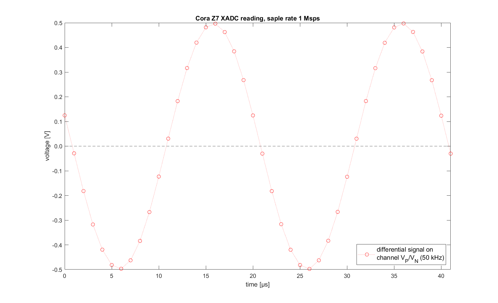
For completeness, let's look shortly also at a practical example using the dedicated analog input channel VP/VN.
The VP/VN channel's AAF cutoff frequency is pretty high at 568.7 kHz. Let's see in the following figure what happens when we feed the inputs with two 50 kHz sine waves of opposing phases and measure the output differentially (the image in full resolution is available here).
There are no surprises. The 50 kHz signal is negligibly attenuated by the AAF, and there is a very slight phase shift in the output.
I reproduced the scenario on a physical Cora Z7 board and measured the signal by the XADC configured to the sample rate of 1 Msps using the software app shared in the repository. The resulting measurement shown in the following figure is exactly as expected. The XADC captures a 50 kHz differential signal with good precision (the image in full resolution is available here).
The Zynq-7000 XADC is equipped with autocalibration capability, which automatically sets Offset and Gain Calibration Coefficients in the XADC registers. XADC may or may not apply these coefficients to the measurements it performs depending on the configuration, which is set by XSysMon_SetCalibEnables().
The XADC performs the calibration automatically at startup. This is because after powering up and during FPGA configuration (i.e., when the bitstream is written into the FPGA or when the PS code is rerun), the XADC starts its operation in so-called default mode. In the default mode, the XADC calibration is done automatically. See details in the UG480, chapter Default Mode.
Even if you change the XADC mode afterward, the calibration done during the default mode will remain valid.
If you need to repeat the calibration later during the runtime (e.g., to make a correction for the temperature changes of the board), you can do that by initiating a conversion on channel 8. This is a special channel that is not connected to any analog input.
The XADC calibrates using a 1.25 V voltage reference external to the Zynq-7000 chip (if present in the board's circuit) or an internal voltage reference within the Zynq-7000 chip.
Using an external voltage reference allows the board designer to achieve higher precision of XADC measurements.
Important:
There is a "catch" regarding gain calibration:
It shouldn't be used when the XADC calibration is done by internal voltage reference of the Zynq-7000 chip (see details explained here).
This is the case for the Digilent Cora Z7 board, which I use in this tutorial.Zynq-7000 reference input pins VREFP and VREFN are connected to ADCGND on this board. Therefore, the internal voltage reference is utilized for calibration.
You need to correctly handle this in the PS code, as I explain in the next paragraphs.
When you know exactly what Zynq-7000 board your code will run on, you can hard-code the configuration, understanding whether the external or internal reference is used. See the schematics of your board to check what is connected to Zynq-7000 reference input pins VREFP and VREFN. The internal voltage reference is used if they are connected to the ADCGND (i.e., the ground of XADC circuitry).
Use the following call (after you initialize the XADC instance) when the internal voltage reference is used to enable only the Offset Calibration Coefficient for XADC and Zynq power supply measurements:
XSysMon_SetCalibEnables(&XADCInstance, XSM_CFR1_CAL_ADC_OFFSET_MASK |
                                       XSM_CFR1_CAL_PS_OFFSET_MASK);
When the Zynq-7000 board you are using provides an external voltage reference, then use the following code to enable both Gain and Offset Calibration Coefficients for XADC and Zynq power supply measurements:
XSysMon_SetCalibEnables(&XADCInstance, XSM_CFR1_CAL_ADC_GAIN_OFFSET_MASK |
                                       XSM_CFR1_CAL_PS_GAIN_OFFSET_MASK);
When the Zynq-7000 internal voltage reference is used for the calibration, the calibration of XADC gain is actually not done (only the XADC offset is calibrated). As explained here, the value of the Gain Calibration Coefficient is set to 0x007F in such a case. 0x007F represents the maximum Gain Coefficient of 6.3%. Obviously, letting XADC apply this maximal Gain Coefficient would reduce the precision of digitalization. That is why we need to pay attention to what kind of voltage reference our Zynq-7000 board uses.
We can write an XADC calibration setup code, which is portable between different Zynq-7000 boards, by checking the value of the Gain Calibration Coefficient.
//Read value of the Gain Calibration Coefficient from the XADC register
u16 GainCoeff = XSysMon_GetCalibCoefficient( &XADCInstance,
                                             XSM_CALIB_GAIN_ERROR_COEFF );

u16 CalibrationEnables;
if( GainCoeff != 0x007F ) // True when external voltage reference is used
    // Use both Offset and Gain Coefficients
    CalibrationEnables = XSM_CFR1_CAL_ADC_GAIN_OFFSET_MASK |
                         XSM_CFR1_CAL_PS_GAIN_OFFSET_MASK;
else
    // Use only Offset Coefficient
    CalibrationEnables = XSM_CFR1_CAL_ADC_OFFSET_MASK |
                         XSM_CFR1_CAL_PS_OFFSET_MASK;

//Set the correct use of the calibration coefficients
XSysMon_SetCalibEnables( &XADCInstance, CalibrationEnables );How precise can the XADC measurement be? Judging by my specimen of the Cora Z7, it can be pretty precise when you use averaging.
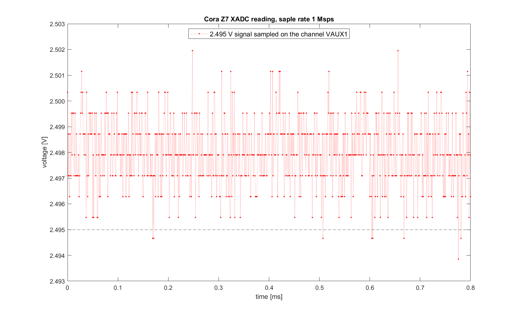
I connected a voltage reference to the unipolar auxiliary channel VAUX[1] of my Cora Z7. My recently calibrated 6½ digits multimeter measured the reference as 2.495 V.
I let the XADC digitize 6400 samples at 1 Msps using the software app shared in the repository. The mean value of the 6400 samples was 2.498 V.
Only a 3 mV difference between a Cora Z7 and an expensive digital multimeter is an excellent result! Mind that the Cora Z7 board doesn't provide an external voltage reference for XADC calibration and that two resistors forming a voltage divider are placed before the VAUX[1] input, i.e., tolerances of the resistors are at play here.
Doing the averaging is no "cheating." Every high-precision voltmeter does the same.
The following figure shows the first 800 samples of my XADC measurement (the image in full resolution is available here).
We see that the noise makes most of the samples oscillate in an interval of 8 bits (8 values) of the 12-bit measurements. One bit represents a 0.81 mV change in the measured voltage.
I mentioned earlier that the XADC can be configured to do averaging of samples. I set 64-sample averaging by calling XSysMon_SetAvg(&XADCInstance, XSM_AVG_64_SAMPLES); and captured 100 samples shown in the next figure (the image in full resolution is available here).
The signal looks much cleaner now. The basic sample rate of the XADC is still 1 Msps, but it averages 64 samples before it produces one sample as the output. Therefore, the apparent sample rate is 15.6 ksps (1000/64 = 15.6). The 100 data points shown in the figure result from 6400 acquisitions done by the XADC.
The output of XADC's averaging is a 16-bit value, so we see much finer differences between the data points compared to raw 12-bit samples in the previous figure.
Of course, you can achieve 64-sample averaging (or any other type of averaging) by post-processing raw 12-bit samples with the PS code or PL logic. Nevertheless, 16, 64, or 256-sample averaging, which the XADC is able to do internally, can save you the coding effort.
DMA (Direct Memory Access)I think the most practical way to transfer large amounts of samples from the XADC for processing in the PS is by means of DMA (Direct Memory Access). This is achieved by including the AXI Direct Memory Access IP in the HW design.
The "magic" of the AXI DMA is that it gets data from the slave AXI-Stream interface S_AXIX_S2MM and sends them via the master AXI interface M_AXI_S2MM to a memory address. If the M_AXI_S2MM is properly connected (as I will show later in this tutorial), the data are loaded directly into the RAM without Zynq-7000 ARM core being involved. (The S_AXI_LITE interface is used to control the AXI DMA by functions from xaxidma.h.)
In essence, you call something like
XAxiDma_SimpleTransfer( &AxiDmaInstance, (UINTPTR)DataBuffer, DATA_SIZE,
                        XAXIDMA_DEVICE_TO_DMA );
in the PS code and wait till the data appears in the DataBuffer (I will explain all the details in a later chapter).
The maximum amount of data that AXI DMA can move in a single transfer is 64 MB (exactly 0x3FFFFFF bytes). This is because the AXI DMA register to store buffer length can be, at most, 26 bits wide.
In our case, we will be transferring 16-bit values, i.e., we can transfer at most 33, 554, 431 samples in one go. That should be more than enough. We could record up to 33.6 seconds of the input signal with the XADC running at 1 Msps.
The XADC Wizard IP can be configured to have an output AXI-Stream interface. When you configure the XADC for continuous sampling, you will get the actual stream of data coming out from the XADC Wizard AXI-Stream interface at a rate equal to the sampling rate of the XADC. However, this data stream is not ready to be connected directly to the AXI DMA.
The thing is that the AXI-Stream interface on the XADC Wizard doesn't contain an AXI-Stream signal TLAST. This signal is asserted to indicate the end of the data stream. The AXI DMA must receive the TLAST signal to know when to stop the DMA transfer.
Therefore, we need an intermediate PL module to handle the AXI-Stream data between the XADC Wizard and the DMA IP. I wrote a module stream_tlaster.v for use in this tutorial.
This Verilog module controls when the data from the slave AXI-Stream interface (connected to the XADC Wizard) starts to be sent to the master AXI-Stream interface (connected to the AXI DMA). This happens when the input signal start is asserted. The module also controls how many data transfers are made (the input signal count defines this) and asserts the TLAST signal of the m_axis interface on the last transfer.
We will control the input signals start and count from the PS (will connect them to the GPIO). First, we set the count, then call XAxiDma_SimpleTransfer(), and lastly, assert the start signal so the data starts to flow into the AXI DMA and thus into the RAM. This will ensure our complete control of how many data samples are transferred from the XADC into the RAM and when.
The next part of this tutorial provides step by step guide for doing the HW design in AMD Xilinx Vivado.


Comments